Business trend:
Nikon allies with
Intel to develop a lithography system that will play a critical role in
manufacturing the next-generation semiconductors. The company plans to put a
technology to halve the production cost of semiconductors by drawing a circuit
on a larger semiconductor wafer than the existing one into practical use by
2018. Intel reportedly decided to bear several tens of billion yen to help
Nikon develop a new lithography system. It has become rather hard for a company
to develop new lithography equipment independently because several hundreds of
billion yen is required for the development. The same is true for the market leader
ASML of the Netherlands that will accept an investment from semiconductor
manufacturers including Intel.
The miniaturization
technology that Intel has been developing under its initiative is reportedly approaching
to the limit. Intel’s strategy to compete Nikon and ASML indicates that further
technological innovation in alliance with equipment manufacturers is critical
for the development of the next-generation semiconductors. Like it or not, the
move to form large syndicates is in progress on the global market. The trend to
establish alliance between semiconductor manufacturers and equipment manufacturers
is supposed to grow widespread in other parts of semiconductor manufacturing
process.
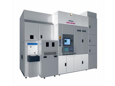
Nikon’s liquid immersion exposure equipment. The competition for technological innovation is heating up in the semiconductor business involving both equipment manufacturers and semiconductor manufacturers.

No comments:
Post a Comment